How to Design the Multilayer PCBs
Multilayer PCBs further increases the complexity and density of PCB designs by adding additional layers beyond the top and bottom layers seen in a double sided configuration. With the availability of over thirty layers in multilayer PCBs configurations, multilayer PCBs allow designers to produce very dense and highly complex designs. Quite often the extra layers in these designs are used as power planes, which both supply the circuit with power and also reduce the electromagnetic interference levels emitted by designs. Lower EMI levels are achieved by placing signal levels in between power planes. It’s also of note that increasing the number of power planes in a PCB design with increase the level of thermal dissipation a PCB can provide, which is important in high power designs.
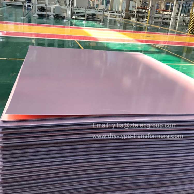
Raw Materials CCL for Multilayer PCBs
In multi-layer PCBs whole layers are almost always dedicated to Ground and Power. So we classify the layers as Signal, Power or Ground planes. Sometimes there is more than one of both Power and Ground planes, especially if the different components on the PCB require different supply voltages.